
The chip nobody talks about but everyone is fighting to buy - inside HBM (High Bandwidth Memory) that controls the pace of global AI chip production, from TSV and interposer technology to the market battle between SK hynix, Samsung and Micron.
When people talk about AI hardware, most think of NVIDIA GPUs. But the component that determines how many of those GPUs can be made and how fast they run is a type of memory called HBM - High Bandwidth Memory.
In 2026, HBM has become one of the scarcest components in the semiconductor industry. Major manufacturers have announced that their entire year’s production capacity is booked solid. The battle between SK hynix, Samsung and Micron has become one of the most-watched stories among investors. This article explains what HBM is, why it matters, and where it is heading.
What is HBM: from narrow road to a thousand-lane highway
HBM is DRAM that stacks multiple memory chip layers vertically and places them right next to the processor on the same package, instead of plugging in as a separate module on the motherboard like conventional RAM.
Imagine memory as a warehouse and the GPU as a factory. Conventional memory like DDR or GDDR is a narrow road where cars drive very fast. HBM takes a different approach: build a massive highway where each car is slightly slower but the total cargo delivered per unit time is many times greater.
The secret lies in three components:
- TSV (Through-Silicon Via) - thousands of microscopic holes drilled through the silicon, acting as vertical wires connecting each DRAM layer
- Base die - the bottom chip that manages data transfer between the DRAM stack and the processor
- Interposer - a silicon substrate with thousands of fine signal traces connecting HBM to the GPU over just a few millimeters
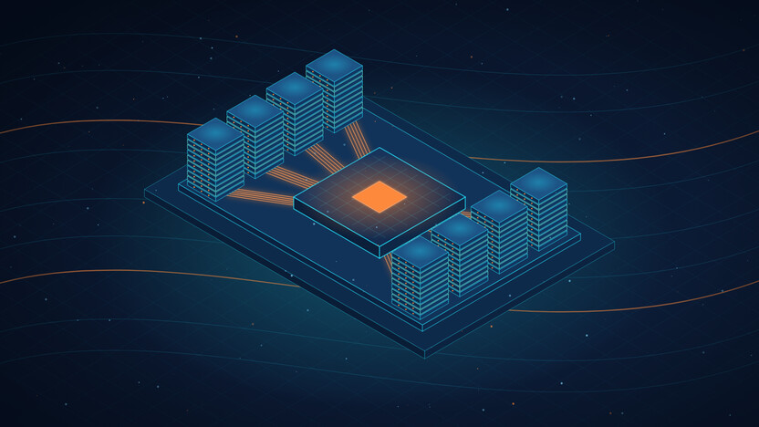
The result: a data bus 1,024 bits wide per stack (2,048 bits in HBM4), compared to just 32 bits per GDDR chip. The short distance also means far less energy per bit, which matters as much as speed in data centers.
The trade-off is cost. HBM is difficult to manufacture, requires advanced packaging, and costs several times more than conventional DRAM. You will almost never find it in gaming GPUs or consumer PCs - but it has become the standard in AI chips and supercomputers.
From the first HBM to HBM4: bandwidth grew 15x in a decade
HBM debuted in AMD graphics cards in 2015 and has evolved through six generations. Each generation increased speed per pin, stacking layers and capacity per stack.
| Generation | Year | Bus width (bits) | Bandwidth per stack | Max capacity |
|---|---|---|---|---|
| HBM4 | 2026 | 2,048 | 2 TB/s | 64 GB |
| HBM3E | 2024 | 1,024 | ~1.2 TB/s | 36 GB |
| HBM3 | 2022 | 1,024 | ~0.8 TB/s | 24 GB |
| HBM2E | 2020 | 1,024 | ~0.46 TB/s | 16 GB |
| HBM2 | 2016 | 1,024 | ~0.26 TB/s | 8 GB |
| HBM | 2015 | 1,024 | ~0.13 TB/s | 4 GB |
Pre-HBM4 figures are approximate from typical specs; HBM4 references the JEDEC standard.
HBM4 is the biggest change since the original. The JEDEC JESD270-4 standard released in April 2025 expands the bus to 2,048 bits, achieves up to 2 TB/s per stack, increases independent channels from 16 to 32, supports up to 16 stacked layers, and reaches 64 GB per stack.
Another game-changer: the base die in HBM4 is manufactured with a logic-chip process, allowing each customer to order custom functionality. HBM is evolving from a commodity into a co-designed component.
Why AI cannot live without HBM: the memory wall
The biggest problem for AI chips today is not compute speed - it is feeding data to the compute units fast enough. The industry calls this the memory wall: GPU processing power has outpaced memory bandwidth for years.
Large language models make this painfully clear. Every time a model generates one token, the chip must read hundreds of gigabytes of parameters from memory. Chatbot response speed depends directly on memory bandwidth. Larger models and longer contexts demand both more capacity and more speed.
This is why AI chip makers pack in as much HBM as possible. NVIDIA’s Rubin platform, which uses HBM4 exclusively, ships with up to 288 GB, and NVIDIA is pushing per-pin speeds beyond 11 Gb/s - about a third higher than the JEDEC standard. AMD’s MI400 uses up to 432 GB of HBM4.
Put another way: a single high-end AI chip uses roughly 8 HBM stacks. Whoever controls HBM production capacity controls the pace of AI chip production worldwide.
The three-player battle: SK hynix leads, but Samsung is catching up
The global HBM market is in the hands of just three manufacturers. In Q2 2026, SK hynix held the #1 spot with 50% revenue share, followed by Samsung at 33% and Micron at 18%, according to Counterpoint Research.
These numbers hide a power shift. A year earlier, SK hynix dominated with 64% while Samsung had only 15% (Counterpoint). The turning point is HBM4:
- SK hynix - the leader since the HBM3 era and NVIDIA’s primary supplier, but faced HBM4 qualification issues that pushed mass production to Q3 2026
- Samsung - trailing throughout the HBM3E era, became the first to ship mass-produced HBM4 to NVIDIA in February 2026, leveraging its more advanced 1c-node DRAM process, and aims to double HBM shipments in 2027
- Micron - the only US manufacturer, confirmed mass-producing HBM4 and already shipping, with this year’s entire HBM capacity sold out
The supply squeeze ripples through the entire memory market. When manufacturers shift production lines to higher-margin HBM, conventional DRAM supply tightens too. The overall DRAM market grew 385% year-over-year in Q2 2026 according to Counterpoint. This impact reaches the RAM prices consumers pay for PCs and smartphones.
Challenges and next steps
Despite the demand, manufacturing HBM at target volumes is not easy. Three main obstacles:
- Yield - more stacked layers means higher probability that any single layer is defective, and one bad layer often kills the entire stack. 12- or 16-layer HBM carries significantly higher cost per good die than conventional DRAM
- Heat and thickness - chip stacks must be thin enough to fit in the same package as the GPU. HBM4 specifies a height of 775 micrometers for both 12- and 16-layer configurations. Manufacturers must grind silicon wafers ever thinner while heat dissipation from middle layers becomes harder
- Packaging bottleneck - HBM is only useful when assembled with a GPU using advanced packaging like TSMC’s CoWoS, which is as supply-constrained as HBM itself
Looking ahead, the industry is targeting HBM4E with even faster per-pin speeds, and hybrid bonding - a copper-to-copper direct chip-attachment technique that enables more layers at lower thickness. The most notable trend is custom HBM, where customers like NVIDIA, Google or AWS design their own base die. Some may even move processing functions into the memory itself, blurring the line between memory manufacturers and logic-chip makers.
Conclusion
HBM is the reason AI chips today are fast enough to train and run large models - and the reason those chips cannot be produced fast enough to meet demand. From a niche technology that appeared in a handful of graphics cards, HBM has become a strategic commodity that shapes the entire industry’s competitive landscape.
2026 is the year HBM4 enters the market and shakes up the leaderboard. The question for next year: will Samsung actually overtake SK hynix? And how will customer-designed HBM reshape the power balance between memory makers and AI giants? Whatever the answer, if you want to understand how fast AI can go, look at the memory - not just the GPU.
Sources
- JEDEC JESD270-4 standard www.allaboutcircuits.com
- ships with up to 288 GB tomshardware.com
- SK hynix held the #1 spot with 50% revenue share, followed by Samsung at 33% and Micron at 18% en.edaily.co.kr
- Counterpoint counterpointresearch.com
- faced HBM4 qualification issues that pushed mass production to Q3 2026 www.trendforce.com
- first to ship mass-produced HBM4 to NVIDIA in February 2026 www.yolegroup.com
- mass-producing HBM4 and already shipping, with this year’s entire HBM capacity sold out en.fnnews.com